
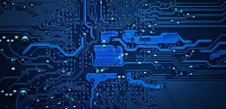
PCB design and engineering—hardware prototyping—is, of course, one of the most important steps in the development process and has been so for a long time now. The creation of the physical prototypes was conventionally a labor-intensive and cost-prohibitive process, having to do with manufacturing techniques and external services. Conversely, 3D printing has been a game-changer in the digital design space of VLSI (Very Large Scale Integration) and PCB (Printed Circuit Board) prototyping.
Fast learning and low prices
One of the main and greatest benefits of 3D-printed models is their quick iteration and refinement. Designers and engineers have the capacity to make physical models of their PCB layouts and enclosures in a matter of hours, which is a great advantage because it facilitates quick evaluation and modification. The process is so fast, which is why it takes less time to market and also makes the workflow more efficient.
However, 3D printing has a lot of advantages compared to the traditional prototyping methods, which are more costly. Material costs are minimal, and expensive molds and setups are eliminated. This allows designers to try out many design iterations without the fear of spending too much money. The scaling of 3D printing enables individuals and small teams to take their ideas to market without the limitation of high expenses.
Unite CAD software and virtual reality.
The incorporation of 3D printing technology and CAD software has completely changed the way engineering hardware and VLSI digital design are done through the process of manufacturing. Most modern CAD software systems have a direct export system that enables designers to move their digital models into physical prototypes with a few clicks.
This integration is very tight, which in turn speeds up the development process by minimizing the possibilities of mistakes and by making sure the representations are correct both in the virtual and physical worlds. Designers can easily visualize and manipulate their ideas, which is very important for understanding how well the designed product will fit and function before entering the final production phase.
Detailed and customizable prototypes
Now, 3D printing technology has reached a level where prototypes with a very high level of detail and customization are achievable. Designers can produce a number of complex mechanical and electrical projects, like hardware pcb design enclosures, intricate mechanical assemblies, and even functional prototypes with integrated electronic components, using the available high-resolution printers and range of materials.
The level of detail and customization at this point lets the designers have the whole ergonomic, aesthetic, and functional aspects of their designs checked, leading to more accurate decision-making and good product quality. Furthermore, through the use of these filaments, e.g., conductive ones, the capacity to fabricate electronic circuits and the networking of the same becomes easier.
Design Verification and Collaboration
Physical prototypes provide a valuable tool in the verification process, and they help the members of a hardware design team communicate better. Physical models give designers the ability to detect problems that may be hard to identify in digital models, including clearance issues, assembly problems, ergonomic challenges, etc.
In addition, 3D-printed prototypes are highly effective in communicating among team members, clients, and stakeholders. Having a real object that displays a design helps build a deeper understanding and lets more productive discussions happen, which in turn leads to improved design stages and better end products.
Bridging Prototyping to Production
Besides 3D printing, technology has also been used to fill the space between designing and manufacturing in particular instances. Thanks to the rapid development of materials and printing technologies, some businesses are now able to print on demand. They have also started to use 3D printing to produce small or specialized batches, which helps to make the production process faster and cheaper.
It is this capacity that makes it possible to manufacture custom parts, enclosures, and even entire products at a speedy pace, thereby addressing market needs quickly and eliminating the chances for design iterations based on customer feedback. The line between prototyping and production is increasingly blurred, which enables the business to take their hardware PCB designs to market even faster.
Environmental Considerations
Not only does 3D printing take the prototyping process to a new level, but it is important to look at the environmental impact of this technology as well. Some 3D printing materials, for example, thermoplastics, could become waste and have the potential to pollute if the recycling process is not well managed.
Nevertheless, the industry is taking action by developing biodegradable and recyclable filaments, reducing material waste, and improving energy efficiency. Through adopting responsible manufacturing processes and sustainable materials, designers and producers will find out how to take advantage of the benefits of 3D prototyping while at the same time reducing their carbon footprint.
Future Advancements and Applications
The combination of 3D printing technology into the hardware PCB design and engineering hardware workflow is only the first step, not the final one. Subsequently, technology is evolving rapidly, so we can expect the next stage of development in material capabilities, printing resolutions, and integration with other emerging technologies, including artificial intelligence and machine learning.
The use of multi-material printing is another promising field of development. It opens up the possibility of building prototypes with different material properties while a single printing process is used. This ability could be used to produce working prototypes with built-in electrical parts, and in the end, this could even result in the blurring of the line between prototyping and manufacturing.
Conclusion
The emergence of 3D-printed prototypes has opened a new chapter of innovative thinking and efficient performance in the world of hardware PCB design and engineering hardware. Through functioning as a rapid prototyping instrument, this technology has offered cost-efficiency and integration with CAD software features that have enabled designers and engineers to bring their ideas to life with previously unseen speed and flexibility.
As the technology continues to evolve, it is very likely that we will have more transformative applications in the digital design in vlsi, PCB development, and such other fields. To sum up, 3D printing adoption for prototyping streamlines the design process and contributes to cooperation, fast production, and sustainable practices.